Photovoltaics: new materials for better efficiency

- The global solar energy market today is 95% silicon-based – although, silicon is not actually the most ideal material for photovoltaic panels because it does not absorb light very well.
- Researchers are looking at alternatives such as thin-film solar cell technology and perovskites.
- Perovskites have now reached the same level of performance as silicon (with an energy conversion of more than 25%), but they are unstable, a problem that still needs to be resolved.
- Photovoltaics in tandem (silicon and perovskites together) are promising since their efficiency can exceed 30%.
Solar photovoltaic (PV) technology has grown almost exponentially over the past 15 years and is now cost-competitive with fossil fuels. Remarkably, the underlying PV structure has remained virtually unchanged since its development at Bell Laboratories in 1954. Indeed, modern solar cells are still based on a simple junction between ‘n’ type (electron-rich) silicon and ‘p’ type (hole-rich) silicon. The first solar cells converted sunlight into electricity with an efficiency of about 5%, a figure that has soared to over 25% in recent years thanks to more sophisticated cell design, namely the addition of highly doped silicon and anti-reflection layers.
Although silicon still accounts for about 95% of the global solar energy market, it has one major drawback: it does not absorb light very well. Large thicknesses of material – to the order of hundreds of microns – are therefore required. Since this is a long distance for electrons to travel, PV-grade silicon must be highly crystalline and very pure for the charge carriers to efficiently pass through. Fabricating such material is complex, however, and therefore expensive.
Changing our approach to silicon
To reduce production costs and the amount of material needed, researchers have long been looking into alternative materials. My team is focusing on thin-film solar cell technology, so-called because the films only need to be a few microns thick for sufficient optical absorption. Lower quality, lower purity materials are also acceptable and they can be fabricated using rapid deposition methods: evaporation, direct-to-glass sputtering or plasma enhanced chemical vapour deposition (PECVD). These materials, which include hydrogenated amorphous silicon, cadmium telluride (CdTe) and copper indium gallium selenide (CuIn1-xGaxSe2, or CIGS for short), make for very efficient cells and can be grown on any type of substrate.
The efficiency of solar cells that convert sunlight into electricity has increased from 5% to 25% in recent years.
Today, crystalline silicon wafers are conventionally fabricated by drawing ingots and then cutting them into wafers about 180 µm thick. We are trying to break new ground in the way crystalline silicon is made by using new growth techniques that rely on low-temperature PECVD processes – that is, between 150 and 300 degrees Celsius. We are also using this technique to make ‘III‑V’ materials which, although widely used in optoelectronics, are about 100 times more expensive than crystalline silicon. In the world of photovoltaics, costs must be reduced to compete with crystalline silicon.
The standard methods for creating III‑V materials are molecular beam epitaxy (MBE) and metal organic chemical vapour decomposition (MOCVD). These epitaxial growth methods require ultra-high vacuum environments for MBE and high temperatures (700‑1000°C) for MOCVD, making them expensive. The plasma deposition processes that we are developing at LPICMt in collaboration with the Institut Photovoltaïque d’Ile de France (IPVF) aim to reduce this cost. This is one of the last variables we have any control over as III‑V compounds are already at the maximum of their efficiency when it comes to converting solar radiation into electricity.
Perovskites: a new material
Perovskites are another class of materials we are working on. These are crystalline materials with the structure ABX3, where A is caesium, methylammonium (MA) or formamidinium (FA), B is lead or tin and X is chlorine, bromine or iodine. They are promising candidates for thin-film solar cells because they can absorb light over a wide range of wavelengths of the solar spectrum thanks to their tuneable electronic band gaps 1. Charge carriers (electrons and holes) can also diffuse quickly and over long distances. These properties mean that perovskite solar cells now boast an energy conversion efficiency of over 25%, putting their performance on a par with established solar cell materials such as silicon, gallium arsenide and cadmium telluride.
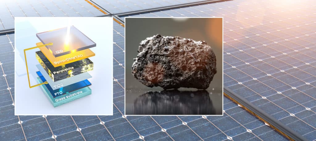
While we know how to make them cheaply and efficiently, the problem is that perovskites contain natural surface defects and suffer from structural changes known as ion migration. Both of these factors tend to make perovskite films unstable and these instabilities become even more pronounced in the presence of moisture and higher temperatures. To improve their stability, we need to understand these materials and the interfaces between the different components that make up the solar cell.
This will be a challenge, but it is worth it, because perovskites are very versatile: their optoelectronic properties can be manipulated quite easily by simple chemical modifications. Thanks to their incredible light absorption capacity, they can be used not only in solar cells, but also in light-emitting diodes and other electronic applications. Research on perovskites is booming and thousands of studies are published every year.
Tandem cells
The next question is: how do we go beyond current efficiencies? While optimising materials and interfaces is crucial, perovskites can also be added to established solar cell technologies (such as silicon) to build so-called tandem solar cells. This is the subject of research at the IPVF and it is an extremely interesting way to increase the overall efficiency of devices. Silicon-only- and perovskite-only cells can both achieve efficiencies of 26%, but if you put them together you can push the efficiency to a higher value (to beyond 30%). Higher efficiencies mean, for example, that you can cover a smaller area with your PV panel to get the same energy output – in other words, it costs less.
Cells made solely of silicon or perovskite can achieve efficiencies of 26%, but together this value can exceed 30%.
So, what are the best materials? If we are able to solve the stability of perovskites, they seem the most promising. III-Vs are also interesting, but we need to reduce their cost. To address climate change, our challenge is to develop terawatts of photovoltaic panels, which means manufacturing large quantities of photovoltaic panels that require large installation areas. Increasing their efficiency while decreasing the thickness of the cells is the best way to reduce the amount of material used.
There are also other problems to be solved, such as recycling the photovoltaic materials and keeping them free of dust so that they can continue to absorb solar radiation efficiently. We are working on the eco-design of solar cells that can be recycled to recover the constituent materials. Photovoltaic plants are in fact precious metal ‘mines’. Perovskites also contain lead, which is toxic and could leach out of a cell in the event of flooding or fire. This aspect of PV technology is a research topic in itself and could be the subject of a future article.